Power Electronics for Embedded Systems & IoT: The Definitive Hardware Engineering Guide
Tuesday, September 22, 2026
01. The Core Dilemma: Why Embedded Hardware Fails in the Wild
In high-reliability embedded hardware engineering, an uncomfortable truth persists: over 75% of unexplainable field failures attributed to "firmware bugs" or "intermittent sensor glitches" are actually direct consequences of violated power integrity. When a microcontroller crashes intermittently, reboots during network transmission, or corrupts its non-volatile memory, software engineers spend weeks debugging RTOS tasks and stack pointers. In reality, the physical silicon is suffocating: supply rails are collapsing below brownout thresholds, ground planes are bouncing during simultaneous switching noise (SSN), or unsuppressed inductive spikes are puncturing sensitive gate oxides.
Unlike pure digital logic or desktop software running on over-provisioned ATX supplies with hundreds of thousands of microfarads of capacitance, an IoT edge node operates in an unforgiving physical environment. It must survive wide input voltage swings, operate from high-impedance batteries, transition between microamp deep-sleep and multi-ampere radio bursts in nanoseconds, and withstand industrial transients—all while packed into dense, cost-optimized printed circuit boards.
1.1 Transients and RF Transmission Burst Droop
Modern wireless SoCs—including the Espressif ESP32, Nordic nRF52/nRF53, and cellular modems like the Quectel BG96 or SIMCom SIM7000—present extreme dynamic load profiles. During deep sleep, an ESP32 draws a mere 5 µA. However, upon waking and initiating RF power amplifier (PA) calibration and 802.11b/g/n transmission, the current demand surges instantaneously to 350 mA – 500 mA within less than 2 µs (di/dt > 250 mA/µs). For cellular IoT modules operating on 2G/GSM or LTE Cat-M1/NB-IoT, the situation is even more severe: GSM transmission bursts demand up to 2.0 A peak pulses for a slot duration of 577 µs.
The instantaneous voltage droop (ΔV_droop) appearing at the microcontroller V_DD pin is governed by Ohm's Law and Faraday's Law applied to the power distribution network (PDN):
Power Rail Dynamic Collapse Equation
ΔV_droop = I_burst × (R_source + R_trace + ESR_bulk) + L_parasitic × (di / dt)
Where I_burst is peak transmission current, R_source is battery/regulator internal resistance, R_trace is PCB trace resistance, ESR_bulk is capacitor equivalent series resistance, and L_parasitic is the loop inductance of the trace and decoupling vias.
Consider a typical lithium thionyl chloride (Li-SOCl2) or standard CR2032 coin cell powering an IoT device directly or via a poorly selected LDO. A fresh CR2032 battery has an internal DC resistance of approximately 10 Ω to 30 Ω, which degrades to over 100 Ω at sub-zero temperatures or as discharge progresses. Attempting to draw a 100 mA burst across a 30 Ω source resistance causes an immediate theoretical voltage drop of:
Numerical Proof of Rail Collapse
ΔV = 0.100 A × 30 Ω = 3.00 V (Total Rail Obliteration)
The rail collapses instantly to zero volts, resetting the microcontroller before a single packet is emitted over the air. Even on systems powered by low-impedance 18650 Li-ion cells, long PCB traces without dedicated low-ESR bulk capacitance suffer inductive rail collapse: a mere 15 nH of PCB parasitic loop inductance combined with an RF burst ramp of 0.5 A in 10 ns yields V = L · (di/dt) = 15 nH × (0.5 A / 10 ns) = 0.75 V of inductive noise alone!
1.2 Brownout Detector (BOD) Trips, Register Corruptions & Watchdog Reboots
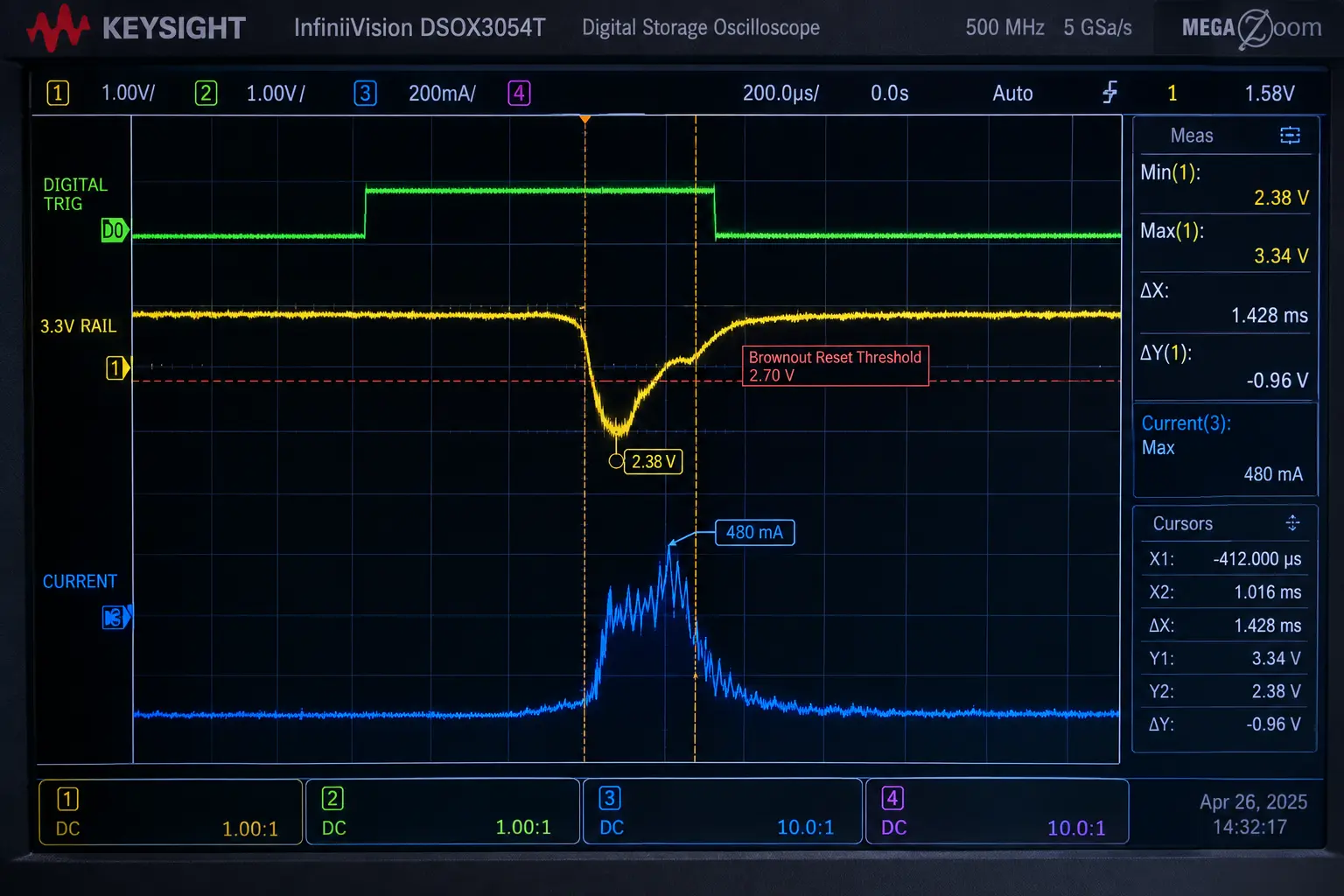
Microcontrollers contain precision internal analog bandgap references and voltage comparators known as Brownout Detectors (BOD) or Power-On Reset (POR) supervisors. In an ESP32 or STM32, the BOD monitors the internal core voltage. If the supply dips below a pre-configured threshold (e.g., 2.43 V or 2.80 V on a 3.3V nominal rail) for as little as 20 nanoseconds, the BOD comparator trips.
This event triggers a severe hardware failure mode known as the Brownout Death Loop:
- The microcontroller boots from cold reset, drawing minimal initialization current (~15 mA).
- Firmware loads peripheral drivers, enters normal execution, and configures the radio module.
- Firmware commands the radio to transmit telemetry. The power amplifier switches on, demanding 400 mA.
- The power rail collapses due to insufficient bulk reservoir capacitance or excessive source impedance.
- The BOD trips, asserting a hard reset signal to the core CPU. The radio abruptly cuts off.
- With the 400 mA load removed, the rail voltage springs back to 3.3V.
- The MCU detects a clean voltage rail and reboots into step 1, repeating indefinitely until the battery is entirely drained.
DANGER: NON-VOLATILE FLASH CORRUPTION MECHANISM
When a brownout trip occurs during an active SPI NOR flash page write or sector erase cycle, the results are catastrophic. Flash programming requires internal charge pumps to boost voltage to 10V – 12V across the floating-gate transistors. If the 3.3V core rail sags mid-write, the internal charge pump collapses, corrupting not only the target data page but frequently destroying the flash status registers or corrupting adjacent sectors. The device becomes permanently bricked in the field, requiring physical desoldering or JTAG repaving.
1.3 Ground Bounce, Ground Loops & Missing Decoupling Loops
A common beginner misconception is that "ground" is an equipotential reservoir of zero volts. In reality, every millimeter of copper trace and every PCB via possesses parasitic inductance:
Ground Bounce Potential Formula
V_bounce = L_GND × (di / dt)
A standard standard-thickness PCB via has an inductance of approximately 1.2 nH. A 10 mm PCB trace typically exhibits 8 nH to 12 nH of loop inductance.
When an 8-bit or 32-bit bus switches simultaneously (e.g., driving high-speed SPI or memory lines from logic LOW to HIGH into capacitive loads), a rapid current surge flows through the ground return path. If this return current must travel through a necked-down ground trace or jump across via stitching, the ground reference of the IC physically bounces upwards relative to system ground. A ground bounce of just 600 mV can cause an adjacent clock line or chip-select pin to cross the V_IL (input low threshold), injecting phantom clock cycles into SPI buses or corrupting I2C packet acknowledge bits.
1.4 Inductive Kickback: Destroying GPIOs and Driver Stages
Whenever an embedded system interfaces with the physical electromechanical world—driving relay coils, solenoids, DC motors, or haptic actuators—it encounters Faraday's Law of Induction. An inductor stores energy inside its magnetic field:
Magnetic Energy Storage
E_stored = ½ × L × I²
Current flowing through an inductor cannot change instantaneously (di/dt ≠ ∞). When a switching transistor (MOSFET or BJT) turns off, breaking the conduction path to ground, the collapsing magnetic field forces the voltage across the inductor to instantaneously reverse polarity in a violent attempt to maintain current flow:
Inductive Back-EMF Equation
V_kick = -L × (di / dt)
If a 12V relay coil with L = 150 mH carrying 100 mA is switched off by a MOSFET in 10 ns, the theoretical voltage spike reaches:
Numerical Calculation of Unclamped Inductive Spike
V_kick = 0.150 H × (0.100 A / 10⁻⁸ s) = 1,500,000 Volts (Bounded only by air arcing & silicon avalanche!)
In practice, the voltage spikes instantly to 80V – 250V, instantly exceeding the absolute maximum V_DS rating of the switching transistor (typically 30V or 60V). The transistor enters catastrophic drain-source avalanche breakdown. The energy discharges through the silicon die, puncturing the sub-micron gate oxide (SiO2) layer and blowing the driving microcontroller GPIO pad into a permanent short to V_DD or ground.
1.5 Inadequate Thermal Management: Turning Linear Regulators into Heaters
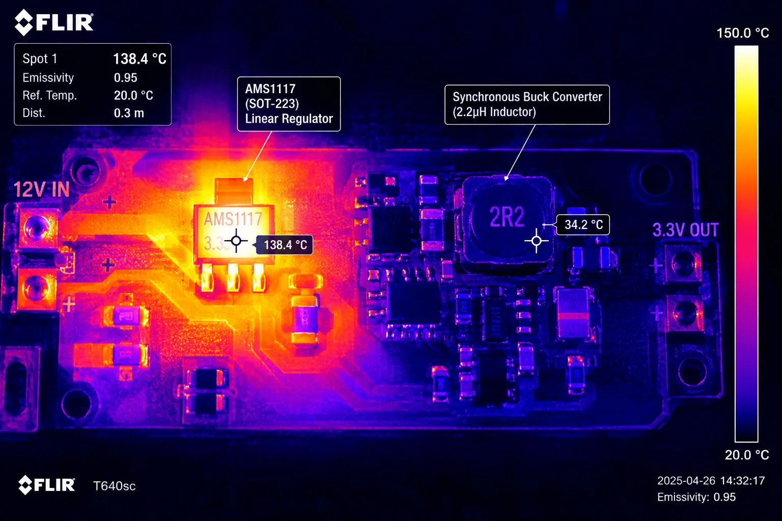
One of the most frequent architectural blunders in embedded hardware design is using a cheap linear regulator (such as the legacy AMS1117-3.3 or LM7805) to step a high input voltage (e.g., 12V or 24V industrial supply) down to 3.3V for a microcontroller.
Linear regulators operate purely on resistive dissipative drop: all excess voltage is converted directly into heat. The internal pass transistor functions as a dynamically controlled variable resistor. The power dissipated as pure heat (P_loss) is:
Linear Regulator Power DissipationHEAT LOSS
P_loss = (V_in - V_out) × I_load + V_in × I_q
The resulting rise in silicon junction temperature (T_J) above ambient temperature (T_A) is calculated via package thermal resistance (θ_JA, junction-to-ambient, expressed in °C/Watt):
Junction Temperature Equation
T_J = T_A + P_loss × θ_JA
WORKED CASE STUDY: THE SOT-223 AMS1117 THERMAL TRAP
Suppose an IoT gateway designer powers an ESP32 (drawing 250 mA average during Wi-Fi operations) from a standard 12V industrial bus using an AMS1117-3.3 in a SOT-223 package (θ_JA ≈ 62 °C/W with typical 1 oz copper PCB footprint):
- Voltage Delta: V_in - V_out = 12 V - 3.3 V = 8.7 V
- Power Dissipation: P_loss = 8.7 V × 0.25 A = 2.175 Watts
- Temperature Rise: ΔT = 2.175 W × 62 °C/W = 134.8 °C
- Junction Temperature at 25°C Ambient: T_J = 25 °C + 134.8 °C = 159.8 °C
The maximum rated silicon operating temperature of the AMS1117 is 125 °C. The IC immediately trips its internal thermal shutdown mechanism (150°C - 165°C), shutting down the 3.3V rail. After cooling for a few seconds, it turns back on, creating an endless thermal oscillation that masquerades as an intermittent firmware crash.
02. First-Principles Voltage Regulation: LDOs vs. SMPS
Every power delivery architecture starts with a fundamental decision: Linear Regulation (LDO) vs. Switched-Mode Power Supplies (SMPS). Making the optimal choice requires dissecting the semiconductor physics inside each topology.
2.1 Linear Regulators (LDOs): Internal Pass Transistors & Dropout Mechanics
A linear regulator consists of four core building blocks: a stable bandgap voltage reference, an error amplifier, a resistive feedback divider, and a series pass element. The type of pass transistor determines the minimum dropout voltage (V_do)—the smallest difference between input and output voltage required to maintain regulation:
Pass Element Type | Internal Topology | Dropout Voltage (V_do) | Quiescent Current Behavior | Phase Margin & Stability |
|---|---|---|---|---|
NPN Darlington | High-side NPN pair driven by collector supply | High: 1.7V – 2.5V | Moderate (5-8 mA), relatively independent of load | Unconditionally stable with virtually any capacitor type |
PNP BJT | Common-emitter PNP transistor | Moderate: 0.3V – 0.6V | Proportional to load: Base current burns I_L / β directly to ground! | Requires output capacitor with specific minimum ESR to prevent oscillation |
P-Channel MOSFET | PMOS pass transistor driven by internal charge pump or rail | Ultra-Low: 50mV – 150mV | Near zero gate current (I_q < 1 µA, down to 25 nA in nanopower devices) | Stable with low-ESR ceramic MLCCs; modern internal pole-zero compensation |
In classic BJT-based regulators like the AMS1117, the pass element is an NPN Darlington. To maintain conduction, the input voltage must exceed the output voltage by at least 1.1 V to 1.3 V. If a battery discharging from 4.2V drops to 4.4V, a 3.3V AMS1117 begins dropping out of regulation, allowing the rail to collapse prematurely. Conversely, modern PMOS LDOs exhibit purely ohmic dropout behavior: at 100 mA, an LDO with an internal pass R_DS(on) = 0.5 Ω maintains perfect 3.3V regulation down to an input of 3.35 V (V_do = 50 mV).
2.2 Quiescent Current (I_q) Benchmarks: The Battery Killer
Quiescent current (I_q), or ground pin current, is the current consumed by the regulator's internal circuitry (bandgap reference, error amplifier bias currents, feedback resistor strings) when delivering zero or minimal load current.
In battery-operated IoT edge nodes that spend 99.5% of their operational lifespan in deep sleep, regulator quiescent current completely dominates battery life:
Regulator IC | Pass Element | Typical I_q | Dropout Voltage (V_do) | PSRR @ 100 kHz | Battery Life Impact (1000mAh Cell, 5µA Sleep MCU) |
|---|---|---|---|---|---|
LM7805 | NPN Darlington | 6,000 µA (6.0 mA) | 2,000 mV | 54 dB | 6.9 Days (Regulator consumes 99.9% of battery!) |
AMS1117-3.3 | NPN Quasi-LDO | 5,000 µA (5.0 mA) | 1,100 mV | 60 dB | 8.3 Days (Completely unacceptable for IoT) |
AP2112K-3.3 | P-MOSFET | 55 µA | 250 mV @ 600mA | 65 dB | 1.9 Years (Standard hobby grade) |
MCP1700 / MCP1702 | P-MOSFET | 1.6 µA | 178 mV @ 250mA | 44 dB | 17.2 Years (Exceeds cell shelf life) |
TI TPS7A02 | P-MOSFET | 0.025 µA (25 nA!) | 145 mV @ 200mA | 62 dB | 22.8 Years (Pure state-of-the-art nanopower) |
Replacing an AMS1117 with a Texas Instruments TPS7A02 or Microchip MCP1700 increases battery life by over 75,000% without modifying a single line of firmware code!
2.3 Switched-Mode Power Supplies (SMPS): Buck, Boost, and Buck-Boost
When the input-to-output voltage delta is large (V_in >> V_out) or input voltage is lower than required (V_in < V_out), Switched-Mode Power Supplies (SMPS) become mandatory. An SMPS uses energy storage components (inductors and capacitors) switched at high frequencies (f_sw ≈ 500 kHz - 4 MHz) to transfer discrete packets of energy with theoretical efficiencies approaching 95% – 98%.
The Synchronous Buck Converter: Operating Physics & Volt-Second Balance
A step-down (Buck) converter consists of an input capacitor C_in, high-side switch Q_1, low-side switch Q_2 (or Schottky freewheeling diode), power inductor L, and output capacitor C_out.
During the ON-state (t_on = D · T_s), Q_1 is closed and Q_2 is open. The voltage across the inductor is:
Inductor State During ON-Time
V_L(on) = V_in - V_out = L × (di_L / dt)
Inductor current ramps linearly upwards at a rate of (V_in - V_out) / L.
During the OFF-state (t_off = (1 - D) · T_s), Q_1 opens and Q_2 closes. The inductor voltage reverses to maintain current:
Inductor State During OFF-Time
V_L(off) = -V_out = L × (di_L / dt)
Inductor current ramps linearly downwards at a rate of -V_out / L.
Under steady-state conditions in Continuous Conduction Mode (CCM), the net magnetic flux over one switching period must equal zero. This fundamental theorem is known as the Inductor Volt-Second Balance:
Volt-Second Balance Derivation
∫₀^(T_s) V_L(t) dt = (V_in - V_out) × D × T_s + (-V_out) × (1 - D) × T_s = 0
Dividing by T_s: V_in · D - V_out · D - V_out + V_out · D = 0 ⟹ V_out = D × V_in.
2.4 Inductor Ripple Current (ΔI_L) and Critical Conduction (CCM vs. DCM)
The peak-to-peak inductor ripple current (ΔI_L) is given by:
Inductor Ripple Current Formula
ΔI_L = [ V_out × (1 - D) ] / ( L × f_sw ) = [ (V_in - V_out) × D ] / ( L × f_sw )
In power electronics design, the Inductor Ripple Ratio (K_ind) is defined as:
Ripple Sizing Guideline
K_ind = ΔI_L / I_out(max) ⟹ Optimal Standard: 0.2 ≤ K_ind ≤ 0.4 (20% to 40%)
Choosing K_ind < 0.2 yields a massive, physically bulky inductor with high DC winding resistance (DCR). Choosing K_ind > 0.4 creates excessive AC core hysteresis loss and increases output capacitor ripple stress.
The minimum inductance required for a specific switching frequency and maximum input voltage is:
Minimum Inductance Calculation
L_min = [ V_out × (V_in(max) - V_out) ] / [ ΔI_L × f_sw × V_in(max) ]
CCM vs. DCM Boundary: As the load current decreases, the minimum inductor current approaches zero. The critical conduction threshold is:
Critical Conduction Current Threshold
I_crit = ΔI_L / 2
When I_out < I_crit, the converter enters Discontinuous Conduction Mode (DCM). In synchronous buck regulators, the low-side FET may be turned off to emulate a diode, allowing the converter to enter Pulse Frequency Modulation (PFM) or pulse-skipping mode. This preserves 85%+ efficiency down to microampere load currents!
Video Tutorial: Linear Regulator vs Buck vs Boost Converter
Electronics Reference
Comprehensive engineering breakdown comparing thermal losses, efficiency curves, and scope waveforms between LDOs and switched converters.
2.5 Comprehensive Power Topology Comparison Matrix
The following matrix provides direct trade-offs across all primary voltage conversion architectures used in embedded and IoT designs:
Converter Topology | Conversion Profile | Typical Efficiency | Output Ripple / Noise | PCB Complexity & BOM | EMI Risk | Ideal Embedded Use Case |
|---|---|---|---|---|---|---|
Linear LDO | Step-Down Only (V_in > V_out) | Low to Moderate | Ultra-Low | Minimal | None | Analog front-ends, precision ADCs, audio codecs, low V_in - V_out drops. |
Synchronous Buck | Step-Down Only (V_in > V_out) | High | Moderate | Moderate | Moderate to High | Primary step-down from 12V/24V or USB-C 5V to 3.3V/1.8V for high-current SoCs. |
Boost Converter | Step-Up Only (V_in < V_out) | High | Moderate to High | Moderate | Moderate | Stepping single-cell Li-ion (3.0V-4.2V) or 2xAA (2.0V-3.0V) to 5.0V USB or relays. |
4-Switch Buck-Boost / SEPIC | Universal (V_in ≶ V_out) |
| Moderate | High | High | Automotive cold-crank systems (6V to 40V), battery discharging through 3.3V window. |
Switched-Capacitor (Charge Pump) | Fractional Step / Inversion (e.g. 2x, -1x) | Load Dependent | Moderate | Low | Low | Gate driver level-shifters, RS-232 dual supply generators, ultra-thin wearables. |
03. Subsystem Power Distribution Networks (PDN) & Decoupling Physics
The objective of a Power Distribution Network (PDN) is straightforward yet mathematically challenging: maintain the impedance of the power rail below a specified target impedance (Z_target) across the entire frequency spectrum from DC up to hundreds of megahertz.
Target Impedance Equation
Z_target = ΔV_noise_budget / ΔI_transient_step
If a 3.3V rail allows a maximum transient noise ripple of ±3% (ΔV = 100 mV) during an RF burst current step of ΔI = 1.2 A, the target impedance is: Z_target = 0.100 V / 1.2 A = 0.083 Ω = 83 mΩ across all frequencies!
3.1 Multi-Layer Bypass Networks: The Decoupling Hierarchy
No single capacitor can provide low impedance across 8 decades of frequency. A robust embedded PDN implements a tiered capacitive hierarchy:
- Bulk Energy Reservoir (47 µF - 470 µF): Solid polymer aluminum electrolytic or conductive polymer tantalum capacitors. These handle low-frequency transient demands (10 Hz - 100 kHz) during radio wakeup pulses, compensating for power supply regulator transient response delays (5 µs - 50 µs).
- Mid-Band Decoupling (1 µF - 10 µF MLCC): Multi-layer ceramic capacitors in 0603 or 0805 packages placed near regulator outputs and subsystem power entries. These maintain low impedance across 100 kHz - 10 MHz.
- Local High-Frequency Bypass (0.1 µF, 10 nF, 100 pF MLCC): Ultra-compact 0402 or 0201 ceramics placed directly against the V_DD and Ground pin pairs of the microcontroller (less than 2 mm distance). These supply instantaneous charge during sub-nanosecond internal clock tree switching edges (> 100 MHz).
3.2 Dielectric Physics: The Catastrophic DC Bias Derating Trap
Among embedded hardware designers, failing to account for DC Bias Voltage Derating in Multi-Layer Ceramic Capacitors (MLCC) is one of the most common causes of unstable power supplies and excessive output ripple.
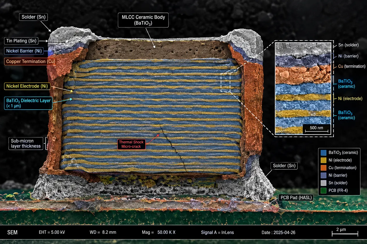
Class II ceramic capacitors (X5R, X7R) utilize Barium Titanate (BaTiO3) as their dielectric material. Barium titanate is a ferroelectric crystalline ceramic. When an external DC electric field (V_DC) is applied across the microscopic capacitor plates, the internal electric dipole domains become forcibly aligned and saturated. Once saturated, they can no longer shift to absorb additional AC voltage charge. The effective capacitance collapses dramatically!
Dielectric Class | Temperature Range | Temperature Stability | DC Bias Derating @ 3.3V (Rated 6.3V, 0603) | DC Bias Derating @ 5.0V (Rated 6.3V, 0603) | Engineering Assessment |
|---|---|---|---|---|---|
C0G / NP0 (Class I) | -55°C to +125°C | ±30 ppm/°C (0%) | 0% Drop (100% True C) | 0% Drop (100% True C) | Perfect linearity. Mandatory for RF matching, filters & timing circuits. Low volumetric density. |
X7R (Class II) | -55°C to +125°C | ±15% max drift | -40% to -55% Drop | Recommended production standard for power decoupling. High reliability. | |
X5R (Class II) | -55°C to +85°C | ±15% max drift | -35% to -50% Drop | -55% to -70% Drop | Acceptable for commercial consumer devices; derate voltage by 2.5x minimum. |
Y5V / Z5U (Class III) | -30°C to +85°C | +22% / -82% | -75% to -85% Drop! | -85% to -92% Drop! | UNUSABLE IN RELIABLE HARDWARE. A 10µF cap becomes a 1.2µF cap under DC bias! |
⚡ HARDWARE RULE OF THUMB: THE 2× VOLTAGE RATING MANDATE
Never specify an MLCC at its nominal operating voltage. For a 3.3V rail, specify capacitors rated for 6.3V or 10V minimum. For a 5V rail, specify 10V or 16V minimum. For a 12V input bus, specify 25V or 50V rated ceramics. Furthermore, physically larger case sizes (0805 vs 0402) exhibit significantly thicker dielectric layers for the same capacitance, drastically reducing internal electric field stress and minimizing DC bias capacitance loss.
3.3 Parasitics: Equivalent Series Resistance (ESR) and Inductance (ESL)
A real-world capacitor is an RLC series resonant circuit comprising the ideal capacitance C, Equivalent Series Resistance (ESR), and Equivalent Series Inductance (ESL):
Real Capacitor Impedance Model
Z(f) = √( ESR² + [ 2π f · ESL - 1 / (2π f · C) ]² )
At low frequencies, capacitive reactance 1 / (2π f C) dominates. At the Self-Resonant Frequency (f_0), capacitive and inductive reactances cancel out, and the impedance dips to its minimum value, equal strictly to the ESR:
Self-Resonant Frequency (SRF)
f_0 = 1 / [ 2π × √( ESL × C ) ]
The Inductive Inversion: Above f_0, the capacitor ceases to behave as a capacitor and becomes an inductor! Its impedance increases linearly with frequency at +20 dB/decade (Z ≈ 2π f · ESL). Placing a 0.1 µF and 10 µF capacitor in parallel creates an anti-resonant parallel LC tank where the inductive slope of the larger capacitor resonates with the capacitive slope of the smaller capacitor. This can create an unexpected high-impedance peak unless damped by moderate ESR or multi-decade staggering.
Video Tutorial: Bypass Capacitors & Power Decoupling Guide EEVblog Engineering Deep Dive
04. Power Switching, Interfacing & Bulletproof Protection Circuits
Embedded systems must safely interface with higher-voltage actuators, peripheral power gates, and external power sources. Without rigorous protection, physical connection events (hot-plugging, reverse polarity, inductive flyback) will destroy semiconductor devices in microseconds.
4.1 Low-Side vs. High-Side Switching: MOSFET Gate Drive Physics
Power switching is bifurcated into Low-Side (switching the load's path to Ground using an N-Channel MOSFET) and High-Side (switching the load's path to V_CC using a P-Channel MOSFET or High-Side N-FET driver):
Switching Architecture | Pass Device | Gate Drive Complexity | Ground Reference Integrity | Critical Pitfall / Failure Mode |
|---|---|---|---|---|
Low-Side Switching | N-Channel MOSFET (e.g. AO3400A) | Trivial | Lifted Ground | Phantom Powering: Connected I2C/SPI lines forward-bias microcontroller internal ESD clamping diodes, causing latch-up! |
High-Side Switching | P-Channel MOSFET (e.g. DMP3035) | Requires Level Shifter | Unified Ground | Gate-source overvoltage (|V_GS| > 20V) under high input voltages requires protective Zener clamping. |
The Logic-Level Gate Threshold (V_GS(th)) Misconception
A frequent mistake when selecting a MOSFET for 3.3V microcontroller control is looking at the datasheet parameter V_GS(th) (Gate Threshold Voltage) and assuming that if V_GS(th) = 2.0 V, a 3.3V GPIO will turn it fully ON.
CRITICAL: V_GS(th) IS NOT THE CONDUCTION VOLTAGE
By JEDEC semiconductor standard, V_GS(th) is defined as the gate-source voltage at which the channel conducts a negligible current of merely 250 µA! At V_GS = V_GS(th), the MOSFET is barely leaving the sub-threshold leakage regime. Driving a MOSFET with V_GS(th) = 2.5 V from a 3.3V GPIO will place it in the linear/ohmic region where its on-resistance R_DS(on) is orders of magnitude higher than rated (e.g. 10 Ω instead of 30 mΩ). Under a 2A load, it dissipates (2 A)² × 10 Ω = 40 Watts, vaporizing within milliseconds!
Staff Rule: Always check the datasheet curve for R_DS(on) vs. V_GS. Only select MOSFETs with guaranteed, specified R_DS(on) tested at V_GS = 2.5 V or 1.8 V (such as the Alpha & Omega AO3400A, Diodes Inc DMG2302UK, or Infineon IRLML2502).
Gate Damping & Pull-Down Networks
A MOSFET gate is an insulated capacitor (C_iss = C_GS + C_GD, typically 200 pF - 2000 pF). Two passive components are strictly required:
- Series Gate Resistor (R_G ≈ 47 Ω - 100 Ω): Placed between the MCU GPIO and gate. Limits peak capacitive charge/discharge current (I_peak = V_GPIO / R_G ≤ 33 mA) to prevent exceeding the microcontroller's maximum pin current rating (typically 20 mA – 40 mA), while dampening high-frequency LC ringing between PCB trace inductance and gate capacitance.
- Pull-Down Resistor (R_PD ≈ 47 kΩ - 100 kΩ): Placed directly between Gate and Source. Prevents the gate from floating in a high-impedance state during microcontroller power-on reset (POR), bootloader execution, or flash programming, which would otherwise allow the MOSFET to partially turn on and burn.
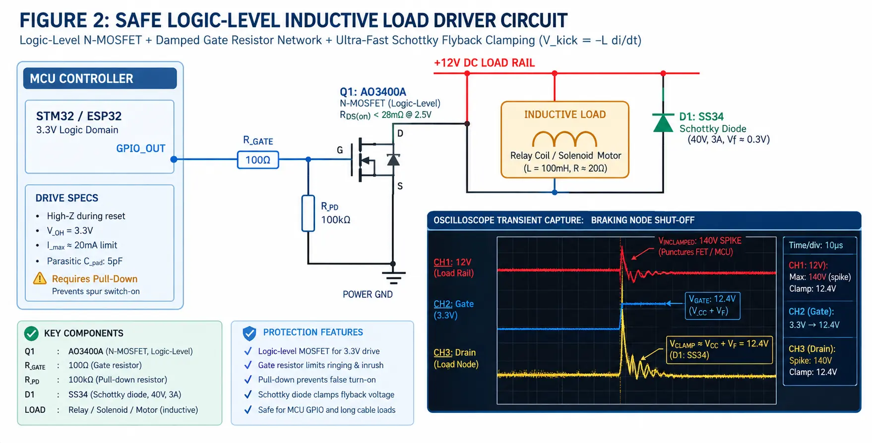
4.2 Inductive Load Clamping: The Reverse Recovery (t_rr) Physics of Diodes
As analyzed in Section 1.4, de-energizing an inductive load generates a severe back-EMF spike (V_kick = -L · di/dt). To safely clamp this voltage, a freewheeling (flyback) diode is placed in anti-parallel across the load (Cathode tied to +V_CC, Anode tied to the MOSFET Drain node).
When the MOSFET turns off, the Drain voltage rises until the diode forward-biases at V_CC + V_F, recirculating the magnetic energy safely through the coil's internal DC resistance until dissipated as heat:
Clamped Drain Voltage
V_Drain(max) = V_CC + V_F(diode)
With a 12V rail and Schottky diode (V_F ≈ 0.4 V), V_Drain is clamped solidly at 12.4V, safely within a 30V MOSFET rating.
WHY THE CLASSIC 1N4007 IS FATAL IN PWM SWITCHING
Many hobbyist schematics specify the standard 1N4001 / 1N4007 silicon rectifier diode for flyback clamping. In DC on/off switching (e.g., toggling a relay once per minute), this works adequately. However, in PWM switching (e.g., motor speed control or solenoid modulation at 10 kHz – 50 kHz), a 1N4007 will destroy your circuit!
The 1N4007 is a standard recovery silicon PN diode with a massive reverse recovery time (t_rr ≈ 2 µs - 30 µs). When the MOSFET abruptly turns back ON, the 1N4007 cannot instantly cease conducting; minority carriers stored in its junction make it conduct in reverse for several microseconds. During this window, the diode forms a dead short circuit directly from +V_CC through the MOSFET to Ground! Massive shoot-through current spikes (> 20 A) flow on every single PWM cycle, causing intense EMI, overheating the diode, and destroying the MOSFET.
Mandatory Solution: Always specify a Schottky barrier diode (e.g., SS14, SS34, BAT54, 1N5819). As majority-carrier devices, Schottky diodes have virtually zero reverse recovery time (t_rr < 10 ns) and lower forward drop (V_F ≈ 0.35 V - 0.45 V).
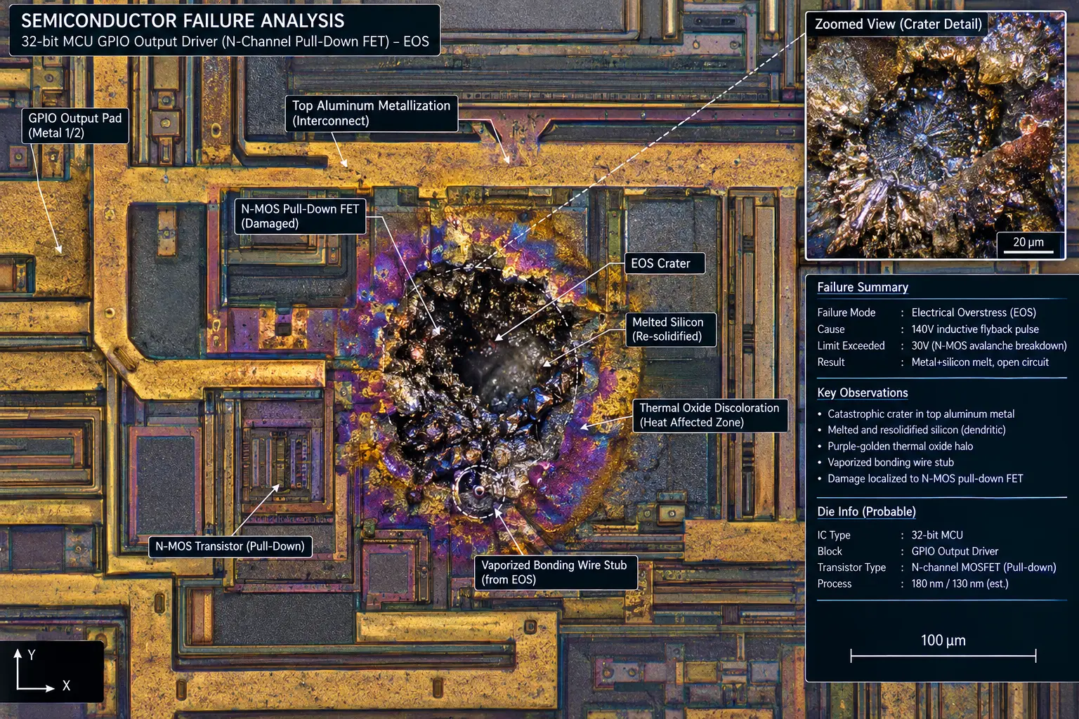
Failure analysis micrograph displaying localized junction burnout caused by unsuppressed relay coil back-EMF discharge
4.3 Galvanic Isolation Architectures: Optocouplers vs. Digital Isolators
In industrial IoT (IIoT) applications—such as Modbus RS-485 interfaces, high-power motor drives, and mains monitoring—galvanic isolation is required to break ground loops and prevent high-voltage surge currents from destroying low-voltage microcontrollers.
Two primary technologies exist:
- Optocouplers (e.g. PC817, 6N137): Use an internal infrared LED optically coupled to a phototransistor. While cheap, optocouplers suffer from Current Transfer Ratio (CTR) degradation over operating temperature and operational life (CTR drops by up to 30% over 5 years of continuous LED illumination). Designers must overdrive the input LED (I_F ≈ 5 - 10 mA), adding significant power overhead.
- Capacitive & Magnetic Digital Isolators (e.g. TI ISO7721, ADI ADuM1200): Use high-voltage silicon dioxide (SiO2) isolation barriers with RF modulation. They consume microamps of supply current, support high data rates (> 100 Mbps), exhibit zero aging degradation, and provide typical isolation ratings of 3.0 kV_RMS - 5.0 kV_RMS.
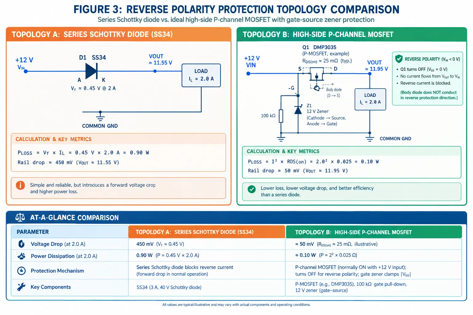
4.4 Input Protection: Reverse Polarity, Polyfuses & TVS Diodes
Reverse Polarity: Schottky vs. Ideal P-FET Circuit
Placing a simple series Schottky diode (such as an SS34) in the power path provides basic reverse polarity protection, but exacts a severe continuous penalty: P_loss = V_F × I_load. At a modest load of 2.0 A with V_F = 0.45 V, the diode dissipates 0.90 Watts as pure heat and starves downstream circuits of 450 mV of headroom.
The Ideal High-Side P-Channel MOSFET Circuit (shown in Figure 3, Panel B) solves this problem entirely:
- The P-MOSFET is connected with its Drain to V_in and Source to V_out (Load), with the Gate pulled to Ground via a 100 kΩ resistor (R_GATE).
- When normal positive voltage is applied, current initially flows through the MOSFET's intrinsic body diode, pulling the Source node up to V_in - 0.7 V.
- Because the Gate is tied to 0V ground, the Gate-to-Source voltage becomes strongly negative: V_GS = V_G - V_S = -(V_in - 0.7 V).
- This negative V_GS fully turns ON the P-MOSFET channel! The ultra-low on-resistance (R_DS(on) ≈ 25 mΩ) effectively shorts out the body diode. At 2.0 A load, the voltage drop is a negligible:
ΔV = 2.0 A × 0.025 Ω = 0.050 V (50 mV), and power dissipation drops from 900 mW down to just 100 mW (an 89% reduction in wasted power!). - Reverse Voltage Behavior: If negative voltage is applied to V_in, the Gate is at 0V and Source is at ground through the load (V_S ≈ 0V). Thus V_GS ≥ 0, keeping the P-FET completely OFF. The intrinsic body diode is reverse biased, completely blocking reverse current flow.
- Zener Gate Protection: Under high input voltages (e.g. 24V bus or automotive surges), V_GS can exceed the maximum allowable gate-oxide limit (typically ±20 V). A 12V Zener diode (D_Z) placed between Gate and Source clamps V_GS to safe levels regardless of input voltage surges.
Overcurrent & Overvoltage: Resettable Polyfuses (PPTC) and TVS Diodes
A comprehensive input stage pairs the P-FET circuit with a Polymeric Positive Temperature Coefficient (PPTC) resettable fuse and a Transient Voltage Suppressor (TVS) diode:
- PPTC Resettable Polyfuse: Composed of a non-conductive polymer matrix embedded with conductive carbon black chains. Under normal current, resistance is low (< 0.1 Ω). When excessive fault current flows, I²R self-heating causes the polymer to undergo a phase transition from crystalline to amorphous, expanding and breaking the conductive chains. The resistance increases by orders of magnitude, limiting fault current to a few milliamps. Once the fault is removed and the device cools, it automatically resets.
- TVS Diode Selection: A solid-state silicon avalanche PN junction designed specifically to clamp high-energy ESD (IEC 61000-4-2) and inductive switching surges in sub-nanosecond response times (< 1 ns). Select TVS diodes based on:
V_RWM(Reverse Standoff Voltage): Must be ≥ normal maximum operating bus voltage.V_BR(Breakdown Voltage): The voltage where avalanche clamping initiates.V_C(Clamping Voltage): Maximum voltage across the TVS during peak surge current (I_PP). Ensure V_C does not exceed downstream IC absolute maximum ratings!
05. Battery Management & Ultra-Low-Power Edge Nodes
Designing battery-operated IoT edge nodes requires mastering both the chemical characteristics of modern lithium cells and the mathematics of active-to-sleep duty cycling.
5.1 Lithium Battery Chemistries & CC/CV Charging Profile
Embedded devices predominantly utilize three distinct lithium chemistries:
Chemistry | Nominal Voltage | Float (Max) Voltage | Discharge Cutoff | Cycle Life | Key Engineering Trade-off |
|---|---|---|---|---|---|
Li-Ion / LiPo | 3.70 V | 4.20 V ± 1% | 3.00 V | 300 – 500 | Highest volumetric energy density. Requires strict overcharge/thermal protection. |
LiFePO4 | 3.20 V | 3.65 V ± 1% | 2.50 V | 2,000 – 5,000 | Incredible thermal stability (zero thermal runaway risk). Extremely flat 3.2V plateau. Lower energy density. |
Li-SOCl2 | 3.60 V (Primary) | Non-rechargeable | 2.00 V | 1 Cycle (15-20 yr shelf life) | Exceptional 10-20 year shelf life (< 1% self-discharge/yr). Requires depassivation pulse handling! |
The Standard CC/CV Charging Algorithm
Charging secondary lithium-ion/LiPo cells safely requires a dedicated four-phase Constant Current / Constant Voltage (CC/CV) charge controller (such as the TI BQ24074 or Microchip MCP73831):
- Pre-Conditioning / Trickle Charge: If cell voltage is < 3.0 V (deeply discharged), fast charging is prohibited to prevent internal lithium dendrite short circuits. The charger applies a gentle 0.1C trickle current until the cell recovers to 3.0V.
- Constant Current (CC) Fast Charge: The charger regulates a constant current (typically 0.5C - 1.0C, e.g. 500 mA for a 1000 mAh cell). Cell voltage rises rapidly from 3.0V toward 4.20V. Approximately 70% of total capacity is replenished in this phase.
- Constant Voltage (CV) Saturation: Once the cell reaches 4.20 V ± 1%, the charger clamps voltage precisely at 4.200V. As chemical absorption saturates, charging current naturally tapers down exponentially.
- Charge Termination: When charging current drops below the termination threshold (typically C/10 or 0.05C, e.g. 50 mA), charging is fully terminated. Trickle floating is strictly avoided to prevent electrode oxidation.
5.2 Deep Sleep Power Budgets: Active-to-Sleep Current Ratios
In typical wireless sensor nodes, active transmission occurs for milliseconds, while sleep lasts for minutes or hours. The true average operational current (I_avg) is calculated as:
Average Duty-Cycled Current Equation
I_avg = [ (T_active × I_active) + (T_sleep × I_sleep) ] / [ T_active + T_sleep ]
Total Operating Life: Factoring in annual battery internal self-discharge (S_D, typically 2% to 5% per year):
Estimated Battery Lifetime Formula
Lifetime (Hours) = [ Capacity_effective × 0.85 ] / [ I_avg + (Capacity_nominal × S_D / 8760) ]
A standard 0.85 derating factor accounts for end-of-life capacity fade and cold-temperature capacity loss.
06. Practical PCB Layout Rules of Thumb for Power Integrity
A schematic only defines electrical connectivity; it does not define spatial electromagnetic realities. A power circuit designed with high-grade components will fail EMC certification or suffer severe jitter if routed improperly.
6.1 Minimizing Critical High di/dt Hot Loops
In switched-mode power supplies, the most critical loop is the High di/dt Hot Loop: the path carrying current that switches abruptly between full load current and zero in nanoseconds.
- Buck Converter Hot Loop: Formed by the input ceramic capacitor C_in, high-side switch Q_1, low-side switch Q_2, and the return ground back to C_in.
- The Magnetic Dipole Radiation Law: The radiated magnetic field emissions (E_rad) scale with the loop area (A), switching frequency (f), and current amplitude (I):
E_rad ∝ A × f² × I. - Staff Rule: Place C_in physically touching the IC V_in and PGND pins on Layer 1. The loop area must be minimized to less than 20 mm². Never route the hot loop through vias to internal layers!
6.2 High dv/dt Switch Node (SW) Containment
The copper connection between the regulator switching pin, inductor terminal, and freewheeling diode is known as the Switch Node (SW). This node toggles between 0V and V_in in 2 to 5 nanoseconds (dv/dt > 5 V/ns).
- The SW node acts as a microscopic transmitting antenna, radiating electrostatic electric fields (E-field EMI).
- Layout Mandate: Keep the SW node copper pour short and wide (to carry inductor current and dissipate heat), but do not make it excessively large. Keep high-impedance feedback traces (FB), analog sensor lines, crystal oscillators, and RF antenna feedlines far away from the SW node.
6.3 Thermal Via Stitching, Solid Planes & Star Grounding
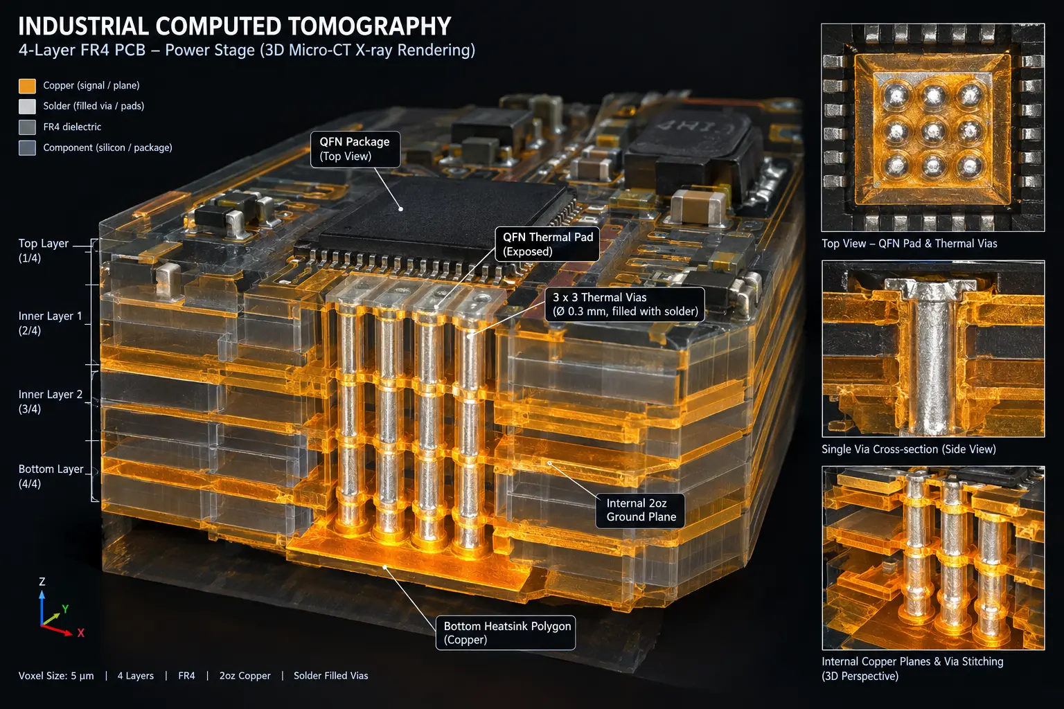
Power regulators dissipate heat primarily through their bottom exposed thermal ground pad (PowerPAD / QFN slug).
- Thermal Via Array: Place an array of 0.3 mm drill vias with 1.0 mm - 1.2 mm grid pitch directly within the exposed thermal pad. Stitch these directly into solid internal Ground and bottom-layer copper planes to conduct heat laterally away from the IC.
- The Myth of Split Ground Planes: In modern mixed-signal boards, do NOT physically slice or split the ground plane with slots! A slot forces return currents to take massive detours, creating huge loop antennas. Instead, maintain an unbroken, continuous ground plane on Layer 2, and achieve isolation through topological zoning: keep noisy power stages on one side of the board and quiet analog sensors on the opposite side.
Video Tutorial: Power Supply Design & PCB Layout Best Practices Texas Instruments Precision Labs
TI engineers demonstrate critical di/dt loops, switch node parasitic capacitance, thermal via arrays, and ground plane return current physics.
07. Curated Open References & Free Engineering Literature
High-authority, free-to-access application notes, design guidelines, and university lecture materials for hardware designers:
Basic Calculation of a Boost Converter's Power Stage
TI SLVA477 The industry-standard reference manual for deriving inductor ripple currents, right-half-plane zeros (RHPZ), output capacitor ESR sizing, and switch FET peak current ratings.
Understanding Buck Power Stages in Switchmode Power Supplies
TISNVA006 Exhaustive mathematical treatment of Continuous Conduction Mode (CCM) vs Discontinuous Conduction Mode (DCM), duty-cycle saturation, and inductor core loss trade-offs.
Basic Calculation of an Inverting Buck-Boost Power Stage
TI SLVA257 Detailed design equations for generating negative voltage rails from positive supplies, including feedback divider calculations and transfer function poles.
Thermal Design Basics & Heatsink Selection
ADI MT-093 Analog Devices tutorial on calculating junction-to-case (θ_JC), junction-to-ambient (θ_JA), and board-level copper dissipation areas.
Decoupling Techniques: Preventing Power Rail Instability
ADI MT-101 Deep physical analysis of high-frequency power supply rejection, local bypass layout, resonance damping, and ferrite bead anti-resonance risks.
MIT OpenCourseWare 6.131: Power Electronics Laboratory
MIT OCW Complete MIT course notes covering magnetic inductor design, transformer core saturation, power semiconductor switching physics, and closed-loop control.
CU Boulder: Fundamentals of Power Electronics (Prof. Robert Erickson)
CU BOULDER World-renowned university curriculum on state-space averaging, AC modeling of switched converters, and magnetic design for power supplies.